This process typically starts with selecting a substrate material, turnkey pcb assembly which is usually fiberglass-reinforced epoxy. Copper foil is then bonded to the substrate, forming the conductive layer of the board. The Gerber files are used to create a photo mask, which is then used to transfer the design onto the copper layer through a process of chemical etching or mechanical milling.
After etching or milling, the board undergoes a thorough inspection to ensure that all traces and connections have been accurately implemented. Any imperfections or defects are corrected at this stage. Subsequently, a solder mask is applied to insulate the traces and protect the copper from oxidation.
One of the final steps is the drilling of holes for component placement and for creating vias that connect different layers of the PCB. These holes are typically filled with conductive material to establish electrical connections between layers. Surface finish processes are then employed to protect the board and ensure the longevity of the connections.
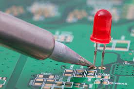
The last phase of PCB fabrication involves assembly, where electronic components are soldered onto the board according to the design specifications. This is a highly precise and automated process that requires advanced machinery to ensure the correct placement and soldering of each component.
In conclusion, PCB fabrication is a complex and meticulous process that forms the foundation of modern electronics. It involves careful design, material selection, manufacturing, and assembly, all of which are crucial for the functionality and performance of electronic devices. As technology continues to advance, so too will PCB fabrication, enabling more compact, efficient, and powerful electronic devices to shape our future.